


Recently, breakthrough research enabled by OptoSeeker Biotech’s flagship product, the OptoBot®500 Optoelectronic Tweezer System, was published in Laser & Photonics Reviews, an internationally renowned journal in laser science and photonics. The study, titled “Tuning Self-Assembled Topological Dipoles in Optoelectronic Traps,” highlights a major advancement in light-controlled topological self-assembly.
I. Laser & Photonics Reviews — A Leading Voice in Laser and Photonics Research
Laser & Photonics Reviews (Impact Factor >13), published by Wiley-VCH, is a highly influential journal covering laser technologies, photonics, micro-/nano-manipulation, and optoelectronic materials. It publishes only original and high-impact research with global scientific relevance.
The inclusion of OptoSeeker Biotech’s OptoBot®500-enabled research in this journal signifies strong international recognition from the academic community and underscores OptoSeeker Biotech’s technical leadership in micro- and nano-manipulation.
II. Research Highlights — Light-Controlled “Magic”: Three Breakthroughs Redefining Micro/Nano Assembly
Conventional micro-/nano-scale self-assembly methods often suffer from limited tunability, minimal dynamic control, and lack of self-recovery, making them unsuitable for precision applications in advanced materials fabrication and bio-manufacturing.
Leveraging the OptoBot®500 Optoelectronic Tweezer System, researchers from Beijing Institute of Technology, OptoSeeker Biotech, and collaborating institutions developed a light-controlled topological dipole self-assembly strategy that achieves three major breakthroughs:
1. Programmable Topological Structures
By tuning optical pattern geometries and electrical parameters, microspheres can be induced to form triangular, square, hexagonal, or other symmetric lattices, as well as undergo topological deformation or phase transitions (Fig. 5 in the original publication).
2. Self-Healing Assembly Systems
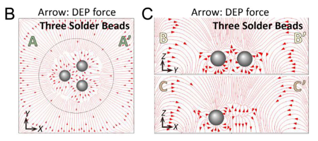
When subjected to external perturbations, assembled structures autonomously return to their original topological configuration driven by restoring dielectrophoretic (DEP) forces—no manual intervention required (Fig. 4).
3. Cross-Material and Cross-Biological Applicability
The strategy works for metallic microspheres, polystyrene (PS) beads, and even yeast cells, demonstrating broad applicability across synthetic and biological systems (Fig. 2).
Compared with traditional optical tweezers, the platform offers lower optical power requirements, high-throughput parallel manipulation, and fully programmable patterns, making it highly promising for micro-/nano-fabrication, optoelectronic materials, bio-assembly, and precision medicine.
III. Methodology — The OptoBot®500 Light-Control Logic: Precision Manipulation via Optoelectronic Traps
The system’s capabilities arise from the deep integration of Optoelectronic Tweezer (OET) technology with principles of topological self-assembly. Its operational logic can be summarized as “Core System + Force-Balance Mechanism + Closed-Loop Workflow”.
(A) Core Technical System
1. OptoBot®500 System Architecture
The setup integrates an upright microscope, a Digital Micromirror Device (DMD) projector, signal generator, and power amplifier. The DMD creates tunable light patterns that project onto a photoconductive layer, generating nonuniform electric fields (Fig. 1A).
2. Optoelectronic Trap Device
The device consists of two ITO-coated glass substrates with a 150-µm spacer forming a 20-µL chamber. The bottom substrate carries a hydrogenated amorphous silicon (a-Si:H) photoconductor, whose impedance distribution—and thus DEP forces—is controlled by projected light (Fig. 1B-C).
3. Multiple Target Types
The system manipulates 20-µm metallic beads (positive DEP), 10-µm PS beads (negative DEP), and yeast cells. Appropriate light patterns (circular, ring-shaped) enable stable trapping (Fig. 1D-E).
(B) Core Mechanisms
-
Projected light induces a nonuniform electric field in the photoconductor, generating dielectrophoretic forces on micro/nano particles.
-
Electrostatic repulsion between particles balances DEP attraction, driving self-organization into symmetric topological structures (Fig. 3B-C).
-
When perturbed, DEP restoring forces return particles to equilibrium positions, enabling autonomous self-healing (Fig. 4G-L).

(C) Manipulation Workflow
-
Load the sample suspension into the device chamber and generate predefined DMD light patterns (circular, ring-shaped, polygonal, etc.).
-
Apply AC voltages (10–30 Vpp, 10–500 kHz) to initiate self-assembly within the optoelectronic traps.
-
Adjust light geometry, pattern size, or voltage parameters to induce deformation or phase transitions, while observing self-healing responses via CCD imaging (Figs. 2, 5).


IV. Experimental Results — Multi-Dimensional Validation Demonstrates System Strength
(A) Topological Self-Assembly: Highly Ordered and Diverse Structures
-
Metallic beads form symmetric clusters of 2–18 particles under circular light patterns, creating triangular, square, pentagonal, or hexagonal lattices (Figs. 2B, 3G).


-
PS beads produce similar ordered arrays under ring-shaped light patterns (Fig. 2D).

-
Yeast cells self-assemble into symmetric configurations, demonstrating biological compatibility (Fig. 2F).

(B) Self-Healing: Rapid Autonomous Recovery
Metallic and PS bead assemblies disrupted by pattern movement return to their original configurations within seconds once the disturbance stops (Fig. 4C-F).
Simulations confirm that DEP restoring forces maintain dipole symmetry and drive recovery (Fig. 4H-L).
(C) Topological Control: Flexible and Tunable
-
Pattern geometry changes (triangular, square, pentagonal) induce reversible topological deformations with preserved connectivity (Fig. 5B-D).

-
Voltage amplitude or pattern size tuning adjusts inter-particle spacing (Fig. 5E-H).

-
Rapid geometry transformations trigger topological phase transitions (e.g., square → mixed → triangular lattices) (Fig. 5I-J).

This publication not only highlights OptoSeeker Biotech’s leadership in optoelectronic manipulation but also showcases China’s innovation capabilities in micro-/nano-technology. With ongoing commercialization of the OptoBot®500, the platform is poised to drive breakthroughs in bio-manufacturing, micro-/nano-robotics, precision diagnostics, and beyond.
OptoBot®500 Optoelectronic Tweezer System — Product Overview
The OptoBot®500 utilizes Digital Micromirror Device (DMD) projection technology and integrates waveform-generation capabilities, enabling direct manipulation of various micro/nano targets—including metallic particles, dielectric beads, nanomaterials, and cells—without the need for auxiliary hardware.
Paired with the OptoMind®500 control software, users can design custom light patterns and perform precise motion control of micro/nano targets through an intuitive interface.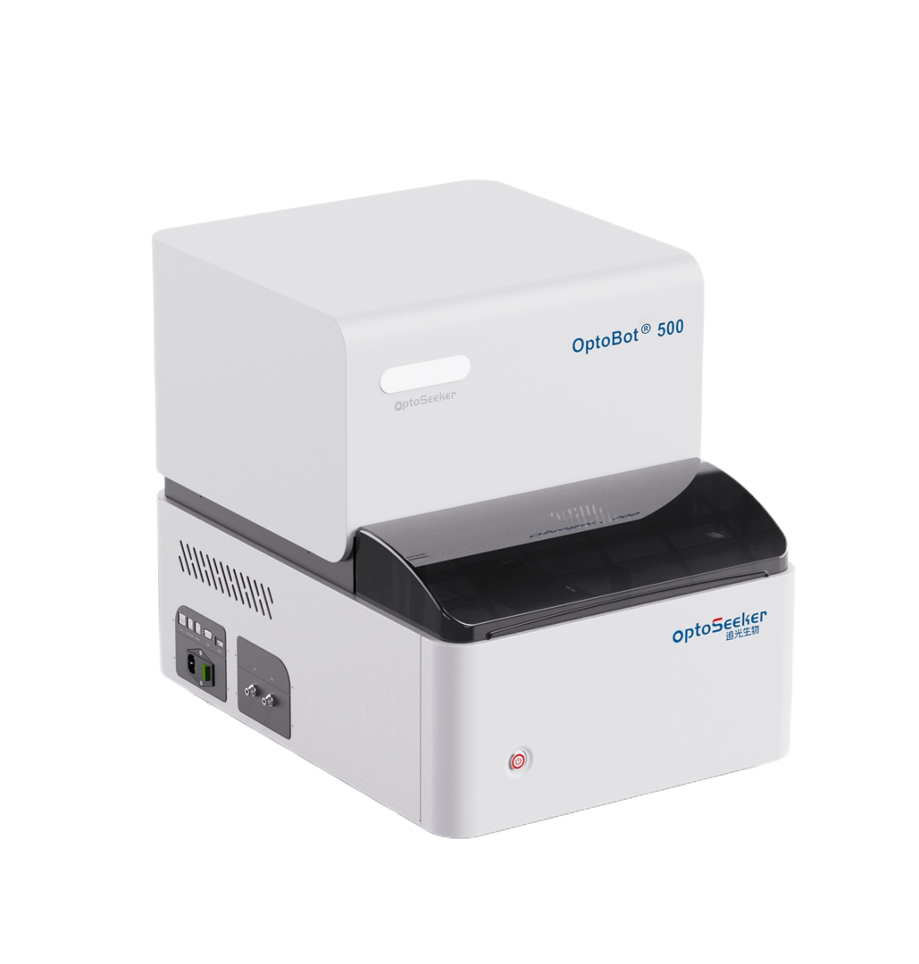 Click to learn more about the product
Original Publication:
Tuning Self-Assembled Topological Dipoles in Optoelectronic Traps
DOI.org/10.1002/lpor.202501697